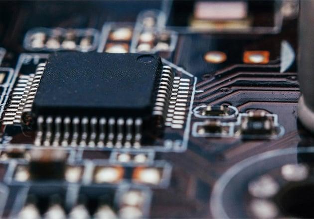
Regardless of your application, whether as a designer of electronic gadgets or hooked to know the details of integrated circuits (ICs), the mastery of your IC chip specifications and data sheets is key. Modern IC chips are unbelievably complicated to assemble, having billions of transistors and revealing the technical details. Yet, deciphering robust chip datasheets as a beginner might sound rather boring and confusing because of the strange language of engineering and parameters.

In this article, we will serve as your guide through the intricacies of IC specifications by breaking down common chip datasheet sections and explaining important parameters and ratings. Our goal is to help you feel more confident in interpreting data sheets next time you need to source an integrated circuit for your project or application. Let's get started!
Components Free Worldwide Shipping
Overview and Introduction
The introduction section provides a high-level overview of the integrated circuit including its:
- Manufacturer name and logo
- Part number or product code
- Commercial/industrial temperature range rating
- Brief description of function
- Block diagram depicting major internal components
The part number includes salient details like manufacturer prefix, device type, package variation etc. Temperature range specifies the rated operating conditions, often industrial (-40°C to +85°C) or commercial (0°C to +70°C) depending on criticality.
Understanding the overall function and subsystems from the block diagram offers context before digging into individual component specifications. Introduction establishes the context before getting into technical nitty-gritty.
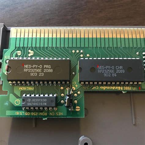
Pinout Diagram
Pins or leads are the physical connection points on an IC package allowing it to interface with the external circuit board or system. The pinout diagram clearly maps:
- Total number of pins on the package variant
- Pin number assigned to each lead
- Pin function described by name or abbreviation
- Common pin assignments color coded
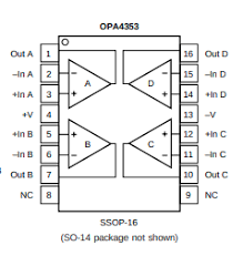
It's essential to verify pin compatibility with your board footprint. Special pins need identification like power, ground, reset, crystal oscillator connections etc. Some complex ICs may have multiple pin variants depending on unused/disabled features.
Always cross-check the mechanical package drawing as well for pin pitch, lead span and IC orientation before physically handling or soldering the component. Correct pin identification avoids drive faults or damage.
Electrical Characteristics
This section defines the key operating parameters of an IC chip at the electrical level:
- Supply voltages - Logic/I/O levels supported, often single or dual power pins
- Current consumption - Peak and average load on power supply
- Digital I/O ratings - High/low input voltage thresholds, output drive capability
- Timings - Clock frequency, propagation delays, pulse widths
- Analog parameters - Operational amplifier specs, ADC bit resolution etc.
Understanding the electrical specifications allows ensuring compatibility with your power source, interfacing devices and expected performance needs from the IC. Out-of-spec conditions may lead to malfunctions.
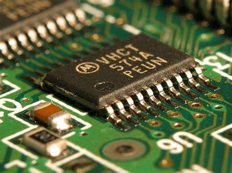
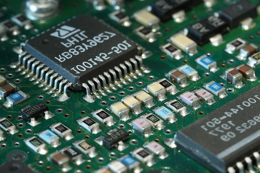
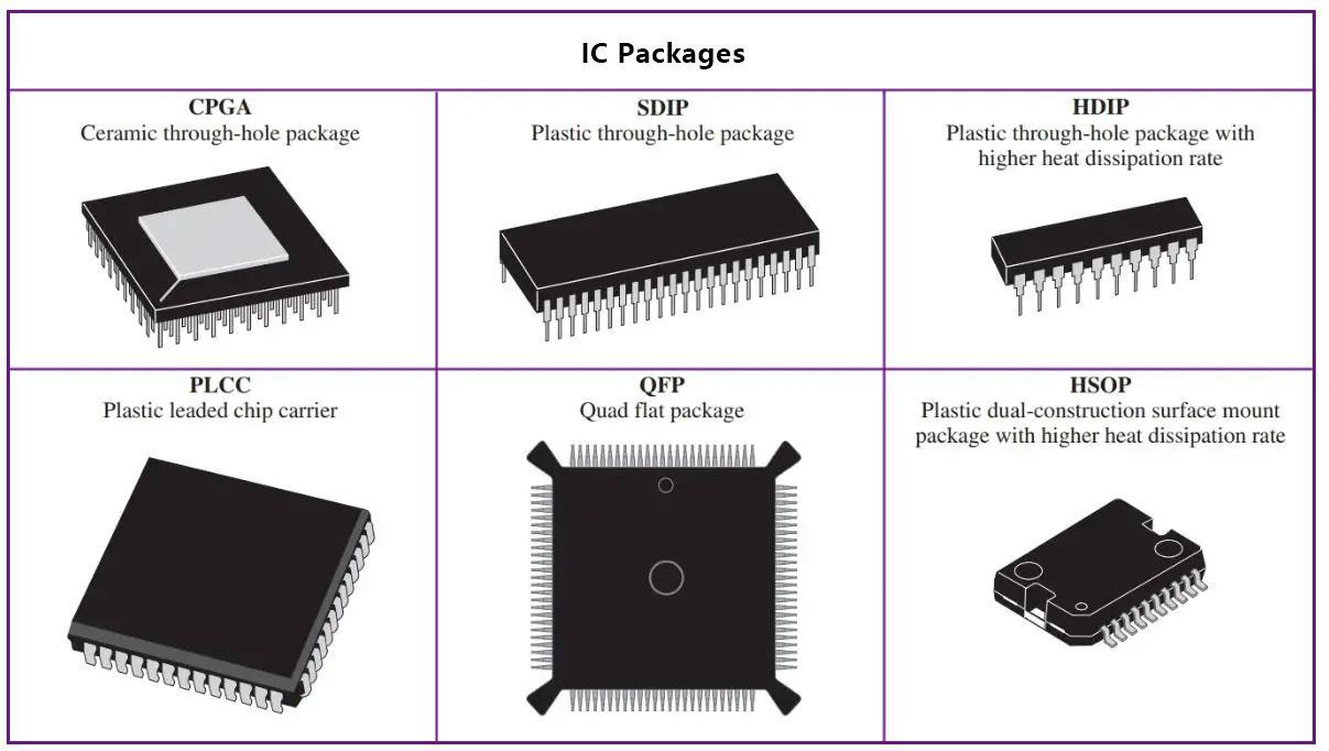
Package Details
Accurately identified the package type is essential as it impacts form factor, mounting style, leads/pins count, thermal management and reliability. Common IC packages include:
- Through-hole mounts (DIP, PIL)
- Surface mount (SOIC, TSSOP, BGA, LQFP)
- Advanced packages (QFP, LGA, MCM)
- Specialty mounts (TO, CERDIP, Side-brazed)
Key attributes include package dimensions, material, lead/pad pitch, pad finish, recommended solder reflow profile and moisture sensitivity level. Proper packaging prevents defects during manufacturing assembly.
Operation Modes
Digital and mixed-signal ICs often support multiple functional modes of operation through software/hardware configuration. Common mode parameters include:
- Active/Idle/Power saving modes
- Programming interfaces - I2C, SPI, UART protocols
- Clock sources and frequencies
- Reset/interrupt pins behavior
- Sample mode rates, triggers, edge selection for ADCs
Understanding available modes helps maximize features/performance while optimizing power consumption for portable applications.
Component Description
Complex ICs contain multiple analog/digital components with unique roles. This section details:
- Component functions like oscillator, filters, amplifiers etc
- Communication protocol cores supported - USB, CAN, Ethernet etc
- Memory capacities - NOR/NAND flash, SRAM, registers
- Processor architecture - RISC/CISC, instruction set, speeds
- Specific analog blocks – ADC resolution, DAC accuracy
In-depth component specifications are essential for algorithms, protocol stacks and system-level requirements validation.
Electrical Characteristic Tables
Crucial numeric operating condition parameters are consolidated into easy-to-reference tables specifying minimum and maximum ratings:
- Supply voltage - VCC, VDD
- Junction temperature - TJ
- Operating free-air temperature - TA
- Input voltage - VIN
- Output voltage - VOH, VOL
- Current per I/O pin - IIO
- Power dissipation - PD
Numbers allow quick checks against design constraints and environmental conditions before proceeding. Safe operating area is critical for reliability.
Application Information
Typical real-world application circuits are illustrated showing recommended component values, interfacing techniques based on industry standards to jumpstart designing.
Schematics demonstrate:
- Supply filtering
- Crystal/RC oscillator circuits
- Reset/power on circuits
- I/O buffer connections
- Sensor interfaces
- Common peripheral integrations
This section handholds new users in prototyping common use cases without tearing through complicated data sheets initially.
Testing & Evaluation
Quality control specs preserve device performance uniformity:
- Production sample testing parameters
- Standard environmental stress screenings
- Burn-in test conditions and duration
- Final electrical parameter verification limits
Knowing test procedures instills confidence in silicon quality and function across operating range. Reliability data may provide MTBF projections also.
Package Marking Information
Physical chip markings allow:
- Identification of manufacturer, part number
- Date/lot code tracing defective batches
- Handling/storage precautions like moisture sensitivity
- Orientation guidelines for pick-and-place machines
Clear marking guidelines ensure correct chip identification during logistics and assembly.
Recommendations
Best practices to optimize IC integration and lifetime:
- PCB design layout guidance
- Supply decoupling capacitor values
- Thermal vias for heat dissipation on dense boards
- ESD/overvoltage protection techniques
- Storage/reflow reflow handling procedures
Following expert recommendations prevents issues from design to field failures.
Traceability Information
Traceability data is critical for:
- Managing military/aerospace supply chain compliance
- Recalling products in case of silicon bugs/issues
- RMA and warranty support activities
Paper trail information on manufacturing plants, shipment dates, wafer lot codes facilitates quality audits and issue root cause analysis when needed.
So in summary, a well laid out datasheet acts as the single source of technical truth offering a holistic understanding of an IC chip right from electrical characteristics and specifications to mechanical drawings, reliability testing procedures, recommended designs/practices. Referring to relevant sections thoroughly ultimately helps maximize performance while avoiding compatibility hazards.
Deciphering Key Specifications
Now that we have examined the typical layout of an IC datasheet, let's look deeper into some important electrical specifications and parameters that require thoughtful consideration:
Supply Voltage (VCC)
This is the positive power supply rail that powers the internal circuitry of digital/analog integrated circuits. Voltage range is typically specified as minimum and maximum allowable input:
- Staying within this voltage tolerance ensures safe operation without current/power exceeding chip limits or risking die damage.
- Lower VCC saves power but impacts maximum operating speed on digital ICs.
- Higher VCC allows greater noise immunity but increases power consumption.
- Dual supplies may be specified for analog/mixed-signal ICs with separate digital and analog rails.
Always use linear regulated bench supplies with sufficient reserve capacity and include decoupling capacitors as per datasheet while experimenting.
Current Consumption (IDD)
Typical and peak current draw numbers allow budgeting power subsystem capacity:
- Average/continuous IDD is important for battery packs and portable devices.
- Peak IDD occurs during processor activity bursts or communication transactions.
- Shutdown/sleep mode IDD helps estimate low power system quiescent current.
- Each active module like flash, ADC, radio is typically documented.
- Pay attention to switching state transitions that spike IDD temporarily.
With experience, average power consumption can be estimated from frequency of use and known mode currents.
Maximum Operating Frequency (fMAX)
Critical speed limitation for microcontrollers, FPGAs and similar real-time clocked ICs:
- Depends on process technology, silicon speed grade and temperature.
- Usually reduces as temperature rises due to carrier mobility effects.
- Understand overhead delays from bus/peripheral access while claiming fMAX.
- Oscillator stability impacts ability to reliably run at edge of spec.
- Allows validation of design meeting clock-driven requirements.
Careful budgeting prevents instability due to race conditions near fMAX limits. Derating accounts for temperature/voltage variation.
Input/Output Voltage Levels
Logic-level compatibility is fundamental for reliable interfacing:
- Typical input HIGH/LOW threshold voltages (VIH, VIL).
- Output HIGH/LOW drive levels (VOH, VOL) under load current.
- Input current (II) must also stay within ratings.
- 3.3V, 5V and various legacy standards exist.
- Avoid exceeding VI ratings during transitions or noise coupling.
Pay attention to I/O types - CMOS, TTL and their differences in voltage/current drives. Ensure all interfacing components meet electrical specs.
Storage Temperature
Long term reliability requires controlling chip temperature:
- Discrete rated TSMAX of 150°C is the standard industry maximum.
- Continuous operating junction temperature TJ(MAX) is lower, often 100-125°C.
- Short term TSTG of -65°C to 150°C allows limited excursions.
- Beyond specifications, accelerated aging and degraded performance will occur over time.
Proper thermal management and derating accounts for worst case ambient temperatures where the device shall last its intended product lifetime.
Mean Time Between Failures (MTBF)
A probabilistic prediction of failure-free operational hours:
- Specified only for military and industrial grade ICs in units of thousands of hours.
- Affected by operating conditions, quality of manufacturing, silicon technology.
- Exceeding ratings decreases actual MTBF below published value drastically.
- Early failures follow exponential distribution but wear out follows normal distribution.
While not a guarantee, MTBF gives a general sense of predicted long-term reliability performance in an application environment.
We hope this detailed guide on understanding IC datasheets has helped demystify some of the confusion around specifications, parameters and ratings. Always review relevant sections thoroughly for any new chip being designed into a project. And when in doubt, check directly with manufacturer support. Knowledge is power, so go forth and master integrated circuit datasheets!
Designing PCBs with Integrated Circuits
Now that we understand what makes an IC tick, let's explore some best practices for physically incorporating them into electronic products through printed circuit board (PCB) design. Proper PCB layout and component placement directly impacts performance, reliability and manufacturability of a design utilizing ICs.
Identifying IC Package Constraints
The physical chip package dictates layout footprint size and joint size/pitch constraints. Factors to consider include:
- Lead/pad pitch - spacing between adjacent pins on sides. Typical 0.05" grid common.
- Lead span - maximum overhang of end leads from package body.
- Pad width/length - compatible with chip size and solder joint volume needs.
- Pad finishes - gold versus HASL, nickel etc. affect joint formation.
- Chip dimensions/shape - long narrow DIP vs compact QFP/BGA.
- Pad count - avoid odd pad counts prone to solder bridging.
- Allowances for manufacturing tolerances.
- Thermal vias - number/spacing determined by package size.
Understanding package constraints early eliminates fit issues during board bring up.
Selecting IC Footprint Symbols
Layout tools provide predefined footprint symbols that:
- Match common package variants like SOIC, QFP, LQFP etc.
- Define pad size, shape, pitch and drill size accurately.
- Include naming conventions identifying manufacturer, device number etc.
- Provide mechanical reference points and fiducials.
Careful selection of the right footprint prevents assembly complications. Custom footprints may be needed for niche variants.
Implementing Power Delivery Structure
Strategically placing decoupling capacitors near each IC:
- 0.1uF X7R 0402 SMD caps for high frequency bypassing.
- 1-10uF Y5V tantalum caps for low frequency ripple rejection.
- Locate as close as possible, less than 0.5" trace distance recommended.
- Use generous copper fill pour under capacitors for low inductance.
- Consider separate analog/digital grounds if mixing signal types.
Proper decoupling eliminates transient voltage variations and noise relatedissues.
Thermal Management Strategies
Dissipating heat is critical to achieve rated performance and lifespans:
- Expose thermal pad underside with vias to internal ground plane.
- Use wide, short traces between IC and vias to minimize thermal resistance.
- space IC packages for airflow either side of the board in enclosures.
- Consider fan/heat sinks if high power ICs are prone to throttling.
- Thermal paste applied between heat spreading components.

Keeping ICs below maximum junction temperature prevents overheating related malfunctions.
Signal Integrity Best Practices
Coupling noises impacts signal integrity, especially high speed lines:
- Separate high speed and clock traces from slower control/power lines.
- Maintain constant trace impedance avoiding etches or splitting traces.
- Terminating transmission lines properly avoids reflections.
- Use parallel pairs of differential traces for signals.
- Add ferrite beads on cables prone to electromagnetic interference.
Preventing noise coupling, crosstalk and reflections is key for reliable communication hardware design.
Electrostatic Discharge Protection
ESD events can damage fragile IC gate oxide layers permanently:
- TVS diodes on all exposed pins clamp transients to safe levels.
- ESD rated connectors at input/output interfaces of boards.
- Anti-static mats and conductive wrist straps handled during assembly.
- Ensure common mode ESD immunity specified for interface ICs.
Follow ESD association guidelines and manufacturer recommendations to safeguard proprietary IC contents.
The concepts covered here pertain to any PCB design incorporating integrated circuits. Careful consideration of electrical interfaces, thermal, electrical loads and protection networks optimize performance while ensuring reliability. With practice, PCB assembly yield also increases through better layout practices.
Supply Chain Management for ICs
Dealing with short lead times, allocation pressures and counterfeit risks presents unique supply chain challenges for integrated circuits. Some best practices include:
Proactive Planning
- Forecast demand across product life cycle and order in batches.
- Select additional supplier sources for critical components.
- Negotiate annual quantity discounts and long term agreements.
Inventory Management
- Categorize ABC components - order high usage items more frequently.
- Balance inventory holding costs versus risk of stock outs and project delays.
- Maintain buffer stocks based on component lead times.
Obsolescence Management
- Track status of ICs through manufacturer change notifications.
- Qualify alternate/drop-in replacement parts ahead of time.
- Maintain long term buy agreements and bank IC quantities.
Counterfeit Protection
- Purchase only from authorized distribtutors with reliable provenance.
- Physically inspect shipment packaging and seals on receipt.
- Perform electrical testing and forensic analysis if doubts arise.
Contract Manufacturers
- Work only with reputed, ITAR compliant EMS partners.
- Perform supplier audits and corrective actions if needed.
- Monitor yields, OTD %, warranty trends of outsourced product lines.
Supply chain visibility and proactive engagements optimize availability while mitigating risks associated with the highly centralized nature of the IC manufacturing industry. This ensures seamless delivery of electronic products.
In summary, a multitude of factors need careful attention right from PCB layout design to supply chain management when working with integrated circuits. Following guidelines set by standards bodies and industry experts helps take full advantage of advanced capabilities ICs offer while avoiding common compatibility headaches
Comment