The statement that smartphones have changed our lives in the last ten years becomes completely clear. These tight-fit miracles provide a wide range of functions from connectivity, games, media and all of these things just within the power of our palms. On the other hand, due to the lightning-fast pace of technological innovations, these new products are a challenge for smartphone manufacturers and even chip designers.
While current smartphone processors deliver incredible performance, consumers demand even faster, more powerful experiences with each new generation. Expanding chip capabilities within the tight space and power constraints of handheld devices requires radical innovation. One pioneering approach gaining momentum is the development of three-dimensional integrated circuits (3D ICs) - once the stuff of science fiction, now poised to reshape the semiconductor industry and propel smartphones to new heights.
The Limits of 2D Chips
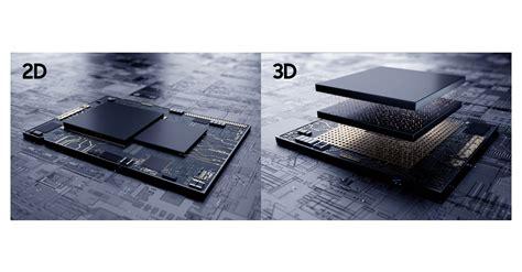
Traditional "two-dimensional" integrated circuits (2D ICs) that power today's smartphones pack billions of transistors into a tiny flat silicon slice. While this approach has fueled exponential processor gains through Moore's Law for decades, fundamental physics limits are now confronting chip designers.
Shrinking transistor dimensions to squeeze more components onto a single plane results in problems like increased power consumption and heat generation. Chips need clever solutions just to maintain reasonable battery life and prevent overheating issues in devices. Additionally, as components are packed denser, signal delays between different parts of the chip slow performance.
Interconnects that link transistor structures together within the planar design also pose challenges. Long metal wiring traces induce resistance and capacitance effects that hamper speed. As circuitry dimensions shrink to the nanoscale, even minor imperfections can cause transistors to malfunction. Yield issues and production costs rise as a result.
With traditional lithography tools nearing their resolution capacities, continuing 2D chip scaling brings sharply diminishing returns. New architectural innovations are required to maintain Moore's Law progress. Three-dimensional integration emerges as a promising approach by stacking and connecting multiple silicon layers in the vertical dimension.
The 3D IC Concept
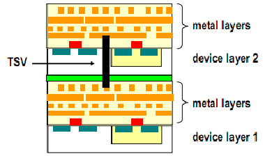
The basic idea behind 3D ICs is to build vertically rather than laterally by stacking active silicon layers and interconnecting them using very short vertical connections known as "through-silicon vias" (TSVs). Each level can contain separate functional blocks like processors, graphics units, memory stacks, and more.
This architecture delivers major benefits over 2D chip design. With components distributed across multiple planes, interconnect delays are reduced since wire lengths shrink dramatically. Thermal issues are also alleviated through increased surface area for heat dissipation. Overall performance can increase while power demands remain unchanged or are potentially decreased.
Moreover, 3D integration allows for heterogeneous integration where different processing elements like CPUs, GPUs, memory, and radio components can be fabricated using separate process technologies and bonded together. Specialized structures optimize for specific tasks rather than a one-size-fits-all planar approach. Increased functional density and performance per unit area become feasible.
While 3D packaging has been utilized in some applications for over a decade, recent breakthroughs now enable true 3D chip stacking with active silicon layers. Precision techniques bond and interconnect ultra-thin wafers or dies with minimal alignment errors. Testing shows 3D designs outperform analogous 2D versions and offer a viable Moore's Law continuation path.
Components Free Worldwide Shipping
3D IC Commercialization Hurdles
Despite major technical progress, several hurdles still impede widespread 3D IC commercialization and deployment in mass-produced consumer devices like smartphones:
Manufacturing Challenges
Fabricating multilayer structures with active components and connecting them vertically is vastly more complex than 2D manufacturing. Yield and reliability concerns exist due to challenges of precisely aligning, bonding, and connecting multiple silicon layers as small as a few microns thick.
Testing Limitations
Traditional product testing methodologies do not easily scale to 3D designs with internal structures. Qualification and debugging of intricate 3D chip designs poses difficulties.
Thermal Management Issues
Heat generated within 3D stacks can more easily concentrate without efficient dissipation pathways. Thermal modeling and mitigation strategies require further refinement.
Packaging Constraints
Device miniaturization demands continue to shrink available space for chip and interconnect packaging. Integrating versatile 3D IC designs within tight consumer product dimensions presents assembly challenges.
Ecosystem Immaturity
Tools, design flows, assembly methods, and other elements of the electronics design infrastructure evolved around planar 2D ICs. Adapting this vast ecosystem for 3D represents a massive change.
While innovations are addressing each concern, overcoming these hurdles demands further development work. Early 3D IC adopters must diligently validate reliability and manufacturability at scale before deploying in mission-critical applications like leading-edge smartphones.
3D IC Industry Progress
Despite barriers, three-dimensional integration R&D rapidly advances due to its potential long-term role in continuing semiconductor performance gains. Major chipmakers, foundries, and packaging firms now heavily invest in 3D IC developments:
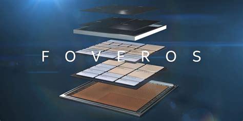
- Intel pioneered earlyThrough-Silicon Via (TSV) technologies and commercialized rudimentary 3D stacking. Its Foveros tech integrates CPUs with GPUs and memory in separate silicon layers connected with many micro bumps.
- TSMC inaugurated its 3D IC Center in 2020 to accelerate innovation. Volume wafer-level production of advanced stacked chips is projected within a few years using InFO and CoWoS technologies.
- Samsung develops technlogies like DX and CoWoS for high density memory stacks. These serve exploding demand for speedy next-gen mobile DRAM and storage.
- AMD, Xilinx, and others leverage TSMC and Samsung foundries. ASIC designers benefit from commercial foundry 3D process offerings.
- IBM, GLOBALFOUNDRIES, and others contribute 3D innovations. GLOBAL's 3DFabric tech hopes to democratize design tools.
- Packaging firms like ASE Group deploy flip-chip and fan-out wafer-level packing methods for 3D ICs.
Despite the slow early pace, initial commercial uses now emerge:
- iPhone 12 models integrate microphone arrays atop sensor hub chips.
- GPU makers stack memory directly atop graphics processors for mobile devices.
- Some HPC/AI accelerators vertically interconnect compute and memory resources for density and performance gains.
As lithographic scaling reaches physical boundaries, a massive transformation integrating the electronics industry around three-dimensional designs appears inevitable over the next decade. Driven by demand for ever-greater power in size-constrained products like smartphones, 3D ICs may finally enable continued exponential gains some thought impossible.
Smartphone Applications of 3D ICs
Smartphones presently drive a massive share of semiconductor industry revenue. As Moore's Law extensions become critical for sustaining product innovation cadences and competitive differentiators, 3D integrated circuit technology appears uniquely poised to propel smartphones to entirely new performance domains. Potential uses of 3D ICs in future handsets include:
Heterogeneous Multi-Chip Packages
Stacking memory such as DRAM onto logic processors like CPUs avoids space-consuming peripheral logic. Enhanced bandwidth and lower power better feed computation-hungry AI/ML apps.
Modular System-on-Packages
Discrete 3D stacked chiplets for cellular radios, displays, cameras integrate functionality more seamlessly while minimizing motherboard area. Space and costs decrease.
Multiprocessor SoCs
3D stacking enables integration of multicore CPUs, GPUs, neural processors, and more for unprecedented system performance within stringent power budgets.
High-Density Storage Solutions
Using through-silicon interconnects, 3D NAND flash memory stacking multiplies available space efficiency over existing 2D designs. Terabyte-class storage seems possible.
Computational Photography
Image processors directly stacked atop large camera sensor arrays eliminate delay-inducing interconnect paths for snappier auto-focus, low light capture, and more.
Embedded AI Acceleration
Specialized AI/ML coprocessors stacked with powerful logic CPUs and high-bandwidth memory promise always-on contextual intelligence far surpassing current discrete smartphone AI chips.
Integrated 5G Modems
System-in-packages tightly couple 5G cellular modem multichip modules with application processors through 3D interconnect reduce board area demands and empower revolutionary cellular experiences.
Thermal Management Gains
Evenly dispersed heat sink pathways made possible with 3D ICs keeps smartphones cooler under the intense workloads of the future without active cooling solutions.
There remains no doubt 3D integrated circuits will profoundly alter smartphone design when challenges of manufacturing, testing and qualification are fully solved. Exciting product innovations may emerge as soon as 2025 as commercial viability matures. For consumers, 3D ICs promise to extend the exponential smartphone revolution well into next decade and beyond.
3D IC Prospects and Conclusions
After decades of anticipated potential, three-dimensional integrated circuits finally reach an inflection point where technical and commercial realities intersect. While formidable obstacles linger, the semiconductor industry now undertakes a massive global effort to fully industrialize this revolutionary technology.
As lithographic and materials limitations increasingly stagnate conventional Moore's Law scaling, 3D integration appears poised to continue the exponential pace of innovation that underpins our increasingly digital world. For in-demand consumer devices like smartphones that push engineering boundaries, three-dimensional designs promise staggering new capabilities within practical power and size constraints.
Innovations in manufacturing processes, metrology tools, thermal design, testing methodologies, software design environments and more all advance at a breathtaking clip. Within perhaps just five years, ubiquitous deployment of 3D ICs in leading-edge applications seems probable. Every facet of the electronics ecosystem transforms accordingly in this tectonic technological shift.
For consumers, the fruits of three-dimensional integrated circuit research translates to more powerful and capable devices delivering richer experiences. Though science fiction just decades ago, stacking active silicon layers now seems the surest path to continuing exponential gains that accelerate and enhance our lives. Where advancements lead remains astonishing to ponder, but 3D ICs ensure exciting frontiers remain ahead in the decades to come. The best is yet to come.
The Dawn of 3D Integrated Circuits
For over half a century, Moore's Law has reliably predicted progress in integrated circuit technology. However, the limits of traditional two-dimensional chip designs now confront semiconductor manufacturers. Three-dimensional integration emerges as the surest path forward to extend Moore's Law into a new era of innovation.
Pushing Physical Boundaries
As transistors shrink to atom-scale dimensions following Moore's Law, physical phenomena like quantum tunneling threaten reliability. Migrating to denser 3D structures avoids issues arising from continued 2D miniaturization. Instead of shrinking laterally, 3D integration builds vertically by stacking silicon wafers or dies and interconnecting them using through-silicon vias (TSVs).
TSVs enable wafer/die stacking pitches only microns apart, far superior to 2D layouts constrained by lithography. Building in three dimensions untethers chip scaling from optical resolution limits and boosts functional density without resorting to exotic new materials. 3D integration prolongs Moore's Law through architecture rather than shrinking alone.
Performance and Power Advantages
Compact vertical interconnects in 3D designs dramatically cut signal transmission delays compared to lengthy 2D global wires. Lower resistance and capacitance means improved power efficiency too. Heat dissipates more readily across increased surface area, easing thermal challenges.
Additionally, heterogeneous integration allows constructing multi-core, multi-function systems optimized instead of general-purpose planar chips. Specialized components like HBM, graphics processors, and AI accelerators tightly coupled via 3D stacking boost performance within strict mobile power budgets.
Mobile and HPC Opportunities
Space and form factor constrained mobile devices driving semiconductor growth benefit immensely from 3D integration. More powerful SoCs with higher density memory and specialized silicon save valuable motherboard area. Thermal constraints ease with heat spreading across layers.
Performance computers also adopt 3D designs. GPU and memory stacks surpass PCIE bus speeds while conserving board space. AI and HPC accelerators highly optimized as 3D packages unleash exponential performance gains within realistic power envelopes.
Manufacturing Realities
While conceptual advantages exist, manufacturing challenges slowed early 3D IC adoption. Yield and reliability risks arise from ultra-precise wafer/die bonding, thinning, and microbump interconnect formation challenging 2D flows. Test and characterization methodology also required reinvention for 3D designs.
However, equipment suppliers now mature key 3D manufacturing technologies. Sematech and the SRC drive infrastructure development worldwide. Early adopters validate important lessons while multi-billion dollar investments transition the overall ecosystem.
A Brighter Future Ahead
With a surfeit of technical and commercial obstacles addressed, true 3D chip fabrication nears mass production scales. Early applications emerged while leading foundries prove high-volume 3D wafer-level processes. EDA tools enable routine 3D design flows, overcoming ecosystem immaturity.
As 3D ICs power flagship smartphones, enthusiasts envision amazing possibilities. Totally new form factors blend silicon with entirely new usage models. Exascale supercomputers may reside anywhere thanks to 3D. The nanoelectronic revolution sparked by 3D integration promises an even brighter technological future than imagined.
The Rise of 3D Chip Stacks
One particularly promising 3D integration approach gaining traction is die or wafer stacking using Through-Silicon Vias (TSVs). Developed through collaboration between IBM, IMEC and others, this interconnect technology uses microscopic vias etched through the silicon wafer or die itself to provide high-density vertical connections.
Die/wafer stacking allows discrete multicore CPUs, GPUs, and specialized silicon like neural network accelerators and image processors to be combined within a single package. Signal delays across these tightly coupled elements decrease exponentially relative to conventional chip packaging. Performance per watt soars accordingly.
Early adopters like Samsung, Intel and TSMC widely apply die stacking in DRAM and flash memory, leveraging the form factor benefits. Stacked memory interfaces use many fewer I/O connections than planar chip arrangements. Taiwanese foundries prove high-yield 200mm and 300mm fabrication for logic and memory die/wafer stacking.
Fan-Out Wafer-Level Packaging
A complementary approach gaining notice is Fan-Out Wafer-Level Packaging (FOWLP), often coupled with die stacking. This technique redistributes fine-pitch solder bump connections across an insulating layer, enabling more compact and flexible designs. Chips require no dicing or packaging overhead until after fabrication.
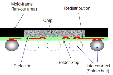
Advantages include reduced manufacturing complexity, higher interconnect density to support 3D stacking, thinner packages, and lower costs. Assembly resembles a 2.5D or 3D-like architecture rather than conventional 2D multi-chip modules (MCMs). ASE, Amkor and JCET pioneered FOWLP adoption making this a mainstream approach.
Early Commercial Adoption
Despite technical and ecosystem challenges, 3D integration now underpins several commercial high-volume applications:
- HBM memory stacked atop GPUs like the AMD Radeon Instinct MI100 delivers 1TB/s+ bandwidth for HPC.
- Stacked DRAM integrated with controllers boosts SSD performance far beyond planar NAND alternatives.
- Apple A12 and A13 SOC packages tightly integrate DRAM in a 3D arrangement for space and efficiency.
- Quad-core mobile SoCs now commonly stack memory directly above logic cores for maximum bandwidth and minimal area usage.
- Intel Foveros stacking logic atop HBM-integrated GPUs foreshadows consumer laptop implementations.
As kinks are addressed and costs decline, expect 3D integration adoption to accelerate rapidly across high-performance computing, mobile, automotive, and beyond in the coming decade.
Continued Innovation
Semiconductor research breakthroughs continually expand 3D integration possibilities. Advanced lithography like EUV enables finer TSV dimensions and tighter stacked die pitch. Copper-to-copper direct bonding obviates expensive intermediate oxide layers. Novel through-substrate vias penetrate both wafer surfaces for extreme densification.
New materials also emerge. Silicon interposers provide routing flexibility between fine-pitch device layers. High-k dielectrics and cobalt interconnects reduce parasitics. Mono-crystalline III-V and graphene transistors lend themselves to 3D integration at scales beyond bulk silicon.
Design automation tools from providers like Cadence, Synopsys and Silvaco fully support 3D flows from early planning through place and route. The 3D ecosystem matures quickly to support a bright future for this revolutionary integration approach. Truly incredible possibilities may emerge as the limits of 3D innovation push well beyond today’s envisioned applications.
Comment